

When Elon Musk presented at the recent TERAFAB event, the ambition was extraordinary: to build 1 TWh of compute capacity per year. Working together, Tesla, SpaceX, and xAI aim to capture a substantial share of the planet’s overall silicon output.
Analysts quickly pointed to ASML as the central constraint. The Dutch company has a monopoly on Extreme Ultraviolet (EUV) lithography systems needed for leading-edge chips, and its backlog extends for years. You cannot simply order a fleet of High-NA EUV machines and expect delivery the following year.
To construct what could be the world’s largest AI hardware operation without being trapped by that bottleneck, the plan combines a newly formed alliance with Intel, a shift toward Gallium Nitride (GaN), and a reimagining of AI chip packaging.
ASML and Modern Chips
ASML is the defining chokepoint for cutting-edge semiconductor manufacturing. It is the only producer of EUV lithography machines, which deploy extremely short wavelengths of light to pattern intricate circuits on silicon wafers.
To build the most advanced logic at dense 3nm or 2nm nodes, EUV is mandatory. Because ASML is the sole supplier and each system requires months to build and calibrate, orders remain backlogged. For a program the size of TERAFAB, waiting years for a fleet of EUV tools is not a practical option.
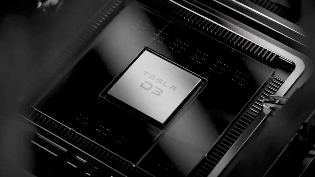
The GaN Chiplet Pathway
A pivotal piece is the partnership between Tesla, SpaceX, and Intel. As that agreement took shape, Intel announced a major advance in Gallium Nitride (GaN) chiplet architecture—closely timed developments.
Intel Foundry unveils the world’s thinnest GaN chiplet (19 μm).
— Intel Foundry (@Intel_Foundry) April 8, 2026
By integrating power and digital control on a single chiplet, it delivers higher efficiency, faster switching, and smaller designs.
Learn more: https://t.co/EvI9UVxktY#IntelFoundry #Semiconductors pic.twitter.com/mEmIWHbXZx
Traditional silicon logic scaling depends on relentless miniaturization to 3nm and 2nm, which requires ASML’s most advanced and heavily backlogged EUV equipment. GaN follows different physics, tolerating significantly higher voltages, temperatures, and frequencies than silicon.
Because of those material advantages, highly efficient GaN chiplets can be built on somewhat more mature nodes using widely available Deep Ultraviolet (DUV) lithography. By prioritizing GaN architectures, TERAFAB can avoid the queue for ASML’s bleeding-edge machines while still achieving major gains in power efficiency.
Radiation Tolerance and Space-Based Compute
The move to GaN also serves SpaceX requirements. Silicon is highly susceptible to radiation, which is why advanced neural networks in space have traditionally needed bulky, expensive shielding.
GaN is inherently radiation-tolerant. By centering the architecture on GaN chiplets, TERAFAB effectively creates off-the-shelf, space-ready hardware. This fits with the broader plan to deploy large, solar-powered xAI data centers in low Earth orbit via Starship, allowing scale-up without straining the terrestrial power grid.
Advanced Packaging Over Node Shrink
Another strategy to bypass the ASML bottleneck is a commitment to "full packages," which includes integrating NAND memory directly alongside compute cores.
Instead of attempting a single, flawless monolithic die on a backlogged 2nm node, TERAFAB employs advanced 3D packaging. Smaller, specialized chiplets can be produced on mature nodes and then interconnected using Intel technologies such as Foveros or glass substrates.
By consolidating logic, power delivery, and NAND memory in a tightly integrated package, data transfer speeds between components increase dramatically.
This approach achieves performance through packaging engineering rather than further lithography shrinking.
Brute Force and Vertical Integration
Scale is a final lever. Companies like Nvidia and Apple vie for ASML capacity because their chips must fit into server racks with strict thermal limits or phones with tiny batteries.
Musk’s method is fully vertically integrated. Tesla and xAI control power generation, cooling systems, server racks, and the software compiler. If a TERAFAB chip is somewhat larger because it was produced on a mature node instead of with an EUV process, that is acceptable: build a larger rack, power it with Tesla Megapacks, and cool it with specialized liquid loops.
By combining Intel’s GaN advances, advanced 3D packaging, and a willingness to meet compute needs with large-scale infrastructure, this plan lays out a path to 1 TWh of compute that avoids ASML’s waiting list.


Share:
2026.2.9.7 Release Notes
Tesla's New LFP Battery Supplier Has Faster Charging Capabilities